

Light Guide Plate Factory Capabilities That Support High Performance Display Backlighting
2026-11-18
Most display backlight failures never start with the LEDs. They start a few millimeters away, inside the light guide plate. That small component decides brightness, uniformity, and whether a high-performance display looks premium or patchy. At Meld Display, light guide plate production is treated as a precision process rather than an afterthought, with factory capabilities built around tight optical tolerances, clean material handling, and repeatable quality control. This post looks at what those capabilities actually mean for display backlighting—and why they matter before the first prototype is assembled.
Micro-pattern etching that keeps brightness uniform across the panel
The etched layer doesn't simply diffuse light the same way across the whole screen. The pattern is denser and slightly deeper near the edges, where light tends to lose energy, and more open toward the centre. That gradual shift evens out the path-length differences that usually leave panels looking brighter in the middle and dull at the borders.
Because the correction is built into the surface itself, it remains consistent whether the display is running at low brightness or full output. There's no extra film stack or electronic compensation to drift over time, and the fine texture stays below the threshold of visibility, so the image keeps a clean, uniform tone without visible banding or patchiness.
Material blends chosen for thermal stability and edge-lit efficiency
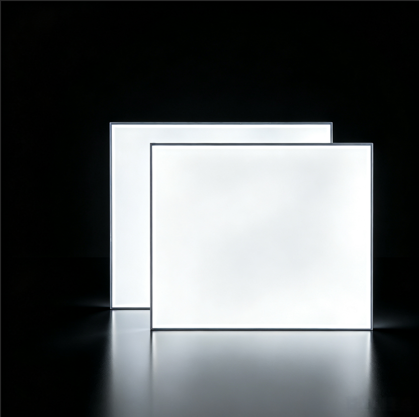
The resin system pairs a high-clarity acrylic base with a small fraction of cyclic olefin copolymer. This combination keeps the light guide's transmission above 92 percent across a 0.5 mm to 6 mm thickness range while raising the deflection temperature enough to survive reflow and prolonged LED board contact. Rather than relying on a single polymer to do both jobs, the blend separates optical duty from thermal duty, so the panel can run at higher drive currents without warping near the injection gate or dimming along the hot edges.
For edge-lit modules, the real test is what happens at the first 20 millimetres from the LED row. A slight haze package, added through the acrylic phase rather than a surface coating, evens out the hotspots without stealing too much axial brightness. The same formulation uses an antioxidant and UV stabilizer pair selected for low migration, which keeps the material from yellowing after thousands of thermal cycles. The result is a cleaner light extraction pattern and less colour shift when the fixture is dimmed or installed in warmer enclosures.
On the processing side, the melt viscosity has been tuned so thin-wall sections fill without excessive shear, which can create stress birefringence and reduce edge-lit uniformity. Molders can run lower barrel temperatures than typical high-heat acrylics, and that helps preserve the reflective film interface and cuts cycle time. The blend is also compatible with laser marking and ultrasonic welding, making it practical for slim luminaire frames where every millimetre of the optical path matters.
In-house optical simulation before tooling begins
We run ray-tracing and photometric checks on the proposed geometry long before any steel is cut. This gives us a clear read on beam spread, cutoff sharpness, and hotspot placement using only the CAD model, so weak zones or glare issues are identified while changes are still inexpensive to make.
The same simulation workflow lets us compare reflector textures, lens curvature, and light guide drafts side by side. Small adjustments to a fillet or a facet angle can be tested in hours, not weeks, which keeps the design loop tight and avoids relying on guesswork once physical parts are already in production.
By resolving optical risks before tooling, the first samples usually arrive much closer to the intended performance. That means fewer mold re-cuts, shorter approval cycles, and a more predictable handoff from the lighting concept to the final part.
Dimensional control that reduces hot spots and dark corners
The lens geometry works at the source instead of trying to fix the beam after it leaves the fixture. By shifting a portion of the forward intensity toward the outer edges, the light no longer piles up in a narrow center while the surrounding area fades quickly. What you get is a cleaner, more balanced spread that still holds its shape across the intended surface.
That balance becomes most obvious in real settings. A countertop or aisle doesn't show a harsh bright spot under the fixture with dim zones at either end, and the eye can move across the space without constantly adjusting to uneven contrast. The result also means fewer fixtures may be needed to cover the same area, since the usable light extends further before losing strength at the edges.
Scalable production without shifting optical tolerances
Scaling production usually exposes tolerance drift that prototype builds hide. In low volumes, a skilled technician can compensate for tool wear, thermal expansion, or subtle fixture movement. Once the line speeds up, those small offsets become systematic errors in surface figure, radius, or centration. A scalable process therefore starts by mapping the tolerance budget onto individual, repeatable operations rather than relying on final inspection to catch drift.
Keeping optical tolerances stable across shifts means placing metrology inside the process loop. Measuring wavefront error or surface irregularity immediately after polishing or molding allows closed-loop correction of pressure, dwell time, or temperature before the next part is made. This approach reduces part-to-part variation not by working faster, but by removing the operator-dependent adjustments and slow environmental shifts that usually separate prototype quality from production output.
Assembly and mounting also deserve the same discipline. Bonding stresses, fastener preload, and cure shrinkage can distort a finished surface even when every optical element measures within specification. Low-stress mounts, thermally matched adhesives, and in-situ alignment checks let the product keep its designed wavefront from first article to full-rate manufacture.
Cleanroom handling that protects light-guide surfaces from micro-defects
Even sub-micron debris can become a visible defect once it lands on a polished light-guide surface. The damage is not always immediate; a particle trapped during assembly can scratch the surface under vibration or thermal cycling, creating scatter sites that reduce total internal reflection and produce dark or bright spots in the finished part. Cleanroom handling therefore treats the surface as the product, not the housing around it, and keeps contact events to an absolute minimum.
In practice, that means operators work with edge grips or vacuum tools rather than touching optical faces, and all tooling is cleaned on the same schedule as the room itself. Static-dissipative trays, ionized air, and low-lint wipes are standard, but the more important control is sequencing: a light guide is removed from protective film only after surrounding assembly steps are complete, so the exposed surface spends the shortest possible time in the air. Glove changes and bench cleaning are logged, which catches contamination trends before they become yield losses.
After handling, surfaces are checked under dark-field or grazing light, where micro-defects show up as isolated points of scattered light rather than as broad haze. The rejection line is deliberately tight for pits, scratches, and adhered particles because even a small mark can appear magnified after the light guide is coupled to a source. Records from inspection feed back into handling rules, so a particular tool, glove lot, or cleanroom zone can be corrected without waiting for a full batch to fail.
FAQ
We combine precision injection molding with laser dot etching and V-cut roll embossing depending on the optical pattern. Injection molding gives us repeatable edge quality for thin panels, while laser work allows variable dot density across the surface to pull more light toward the center of larger screens.
We adjust the optical pattern region by region rather than using a fixed pitch. Dots or microgrooves are placed less densely near the light entry side and more densely toward the far edge. This evens out the luminance profile and often lifts edge-to-edge uniformity above 90 percent.
We routinely produce plates from 0.3 mm up to 2.0 mm, with thickness variation held within ±0.02 mm on most runs. For very thin panels we move to high-flow optical grade PMMA and monitor cavity pressure during molding to avoid warpage.
Yes. We run multi-axis trimming and CNC finishing for rounded corners, notches, holes, and curved edges. The main constraint is keeping the light path intact, so we work with the customer's mechanical layout early to avoid dark zones around cutouts.
Each batch goes through dimensional inspection, surface defect scanning, warpage measurement, and a luminance mapping test using a reference LED array. We also sample optical transmission and yellowing index for materials that will be used in high-temperature environments.
Optical-grade PMMA is the default for most display work because it balances transmission above 92 percent with easy processing. For applications that need more heat resistance or impact strength, we switch to polycarbonate or MS grades, though those usually require adjusted pattern compensation.
It makes a measurable difference. Our mold shop can modify an existing light guide tool within a few days, and new prototypes usually ship in one to two weeks. Because the optical pattern is validated on our own test bench, we avoid the back-and-forth that happens when tooling and optical testing are separated.
We handle pilot lots of a few hundred pieces up to production runs in the hundreds of thousands per month. Consistency comes from cavity-level monitoring and periodic light distribution checks, so the first article and the last article in a run are held to the same specification.
Conclusion
Manufacturing light guide plates that hold up under demanding display backlighting starts long before any mold is cut. The facility runs in-house optical simulation to map how light will travel through each pattern, then translates that data into micro-pattern etching across the panel. Rather than relying on a generic dot grid, the etching depth, pitch, and density are adjusted locally so luminance stays even from the LED input edge to the far corner. This approach also feeds directly into dimensional control: by keeping thickness variation and wedge geometry within a narrow window, the plates avoid the usual hot spots near the light source and dark corners at the opposite side. The result is a backlight unit that looks uniform on first inspection, not only after repeated rework.
Material choice matters just as much as surface geometry. The team works with resin blends formulated for thermal stability and edge-lit efficiency, which means the plate can sit close to high-brightness LEDs without warping or yellowing over time. That stability carries into volume production. As runs scale, process monitoring keeps optical tolerances from drifting, so the thousandth plate behaves like the first. Finally, all handling takes place in a cleanroom environment where contact points, trays, and inspection steps are controlled to prevent micro-scratches or particle contamination that would scatter light. Together these capabilities allow the factory to support thin, high-performance displays without trading optical consistency for output speed.
Contact Us
Contact Person: Sky Wang
Email: [email protected]
Tel/WhatsApp: 8613430620125
Website: https://www.meldled.com/